Tempe, Ariz.—August 14, 2019—Deca Technologies, a wafer-level electronic interconnect solutions provider to the semiconductor industry, today announced that Industry researchers, Yole Développement, and TechInsights have independently confirmed that M-Series™ fan-out wafer-level packaging (FOWLP) technology created by Deca Technologies has been adopted by Qualcomm for power management integrated circuit (PMIC) devices in Samsung’s flagship S10 handset, along with the Xiaomi Mi 9 and LG G8 handsets.
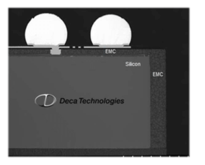
A remarkable development within the initial application is the use of M-Series fan-out technology to create a “protected fan-in WLCSP” where all the solder balls remain within the silicon area. Deca’s patented M-Series structure and methods are used to encapsulate the active semiconductor side and four surrounding vertical sidewalls of the device. Additionally, Deca’s patented Adaptive Patterning™ technology is used in the design and manufacturing processes.
Utilization of Deca’s M-Series processes to encapsulate and protect the device allows both integrated circuit (IC) producers and original equipment manufacturers (OEMs) to approach zero defects related to silicon cracking or chipping.
Sidewall chipping of conventional fan-in wafer-level chip-scale packages (WLCSPs) remains a key quality concern for cell phone OEMs and IC companies throughout the supply chain. Chipping or cracking defects can arise during device singulation, in shipping or in the board mounting process due to the exposed silicon. Adopting M-Series FOWLP mitigates this problem.
“A growing community of semiconductor customers and end electronic product OEMs is taking notice of the benefits that M-Series can provide. Outstanding board level reliability performance coupled with extreme miniaturization vs. competing alternatives is the starting point,” said Garry Pycroft, VP Sales & Marketing at Deca Technologies. “The fully protected nature not only drives elimination of silicon cracking and chipping, it also provides benefit for light-sensitive devices, blocking over 10X the ambient light compared with conventional fan-in WLCSP. Radio frequency device users also see improved electrical performance capabilities with the unique dielectric structure between the active device and redistribution layers.”
A cross-sectional image of a protected fan-in device recently built at Deca Technologies’ Philippines location is shown below.
With noted success in the low-density fan-out market, Deca is working to scale its M-Series and Adaptive Patterning™ technologies to support the anticipated strong growth of chiplets and heterogeneous integration. In the near future, Deca’s unique approach will allow scaling in both directions simultaneously: scaling up from 300mm round to 600mm square manufacturing format while also scaling down from 8µm line and space (l/s) to below 2µm l/s.
For more information on M-Series, please visit: M-Series
About Deca Technologies
Founded in 2009, Deca Technologies is an electronic interconnect solutions provider offering advanced interconnect foundry services to the semiconductor industry. Headquartered in Tempe, Arizona with high-volume manufacturing in Asia, Deca Technologies is a privately held company with leading investors including Cypress Semiconductor Corp. (NASDAQ: CY), ASE Technology Holding Co., Ltd. (NYSE: ASX), Qualcomm Ventures (NASDAQ: QCOM) and SunPower (NASDAQ: SPWR). Deca’s mission is to deliver an exceptional customer experience through its proprietary and transformative electronic interconnect technology. Integrating its solar and semiconductor background, Deca leverages unique equipment, processes and operational methods to break down traditional barriers in the continued adoption and growth of next-generation wafer-level electronic interconnect. For more information, please visit www.decatechnologies.com.
Deca Technology Company Contact:
Garry Pycroft
VP Sales and Marketing Partner
Deca Technologies
Tel + 1 480 345 9895
[email protected]


